Naval Research Labs Helping PowerAmerica Members Identify Materials Defects; Improve Wafer Yield and Device Reliability
Naval Research Labs (NRL) has been using its advanced non-destructive ultraviolet photoluminescence (UVPL) wafer mapping capability to provide Basal Plane Dislocation (BPD) and other material defect mapping to PowerAmerica member companies including X-Fab, GeneSiC and SemiQ. These material defects adversely affect device yield and reliability. The maps and analysis provided by NRL have helped these companies identify and suppress these defects.
Within the PowerAmerica program, NRL initiated a collaboration with X-Fab to investigate the introduction of BPDs due to Al implantation. This work showed that BPDs introduced by implantation of Al required the combination of room temperature implantation and activation anneal. It also showed a strong dose dependence: the dose used for p-wells did not introduce BPDs, whereas the higher dose for p+-contacts consistently introduced BPDs.
These findings led to the creation of another DOE program, “Improving SiC Wafers and Processing for Lower Costs and Higher Reliability.” For this program, NRL is working with NREL, Microchip, SUNY Polytechnic Institute, The Ohio State and Auburn University to determine the feasibility of using room temperature (RT) Al implantation to manufacture reliable SiC MOSFETs. MOSFET fabrication is being done at X-Fab and another SiC foundry. The attraction of RT Al implantation is that the overall cost to fabricate SiC MOSFETs is significantly lower.
In addition to expanding domestic production of high-yield and reliable SiC devices for today’s market, PowerAmerica has addressed key issues concerning the expansion of SiC devices in the future power electronics market. SiC devices have the innate potential to outperform Si devices in the higher voltage range, > 15 kV, such as would be needed for microgrid systems. Bipolar devices such as IGBTs will be needed for these applications, and they will need thick epitaxial drift layers, > 150 µm. To optimize the trade-off between on-state and switching losses, it will be necessary to enhance and to control the carrier lifetime throughout the whole drift layer.
One of NRL’s accomplishments within PowerAmerica has been to work with Wolfspeed/Cree to demonstrate the capability of the non-destructive technique developed by NRL to measure carrier lifetime through thick epitaxial layers such as is required for high-voltage IGBTs. Techniques presently used to monitor lifetime only sample the lifetime to about 50 µm deep. The study with Wolfspeed/Cree shows that NRL’s non-destructive technique provides the capability to measure lifetime over the full drift layer thickness and at depths over 150 µm. Thus, it has the capability to guide the development of the processing steps for enhancing and maintaining the high carrier lifetime required in the IGBT drift layer.
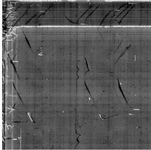
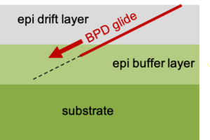
Example of BPDs introduced by aluminum implantation and activation anneal during the fabrication of PiN
diodes: (a) is a UVPL image BPDs introduced by the processing (yellow arrows point to some of them) and (b) is a
schematic showing how BPDs originate from small defect areas in or near the top implanted layer and glide
towards the substrate along basal planes. In (a) the metal contacts were removed to do the UVPL imaging.